| CPC H01L 23/60 (2013.01) [H03F 3/195 (2013.01); H03F 3/245 (2013.01); H03F 2200/318 (2013.01); H03F 2200/441 (2013.01); H03F 2200/451 (2013.01); H03F 2200/541 (2013.01)] | 23 Claims |
|
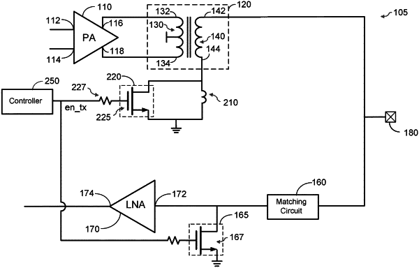
1. A chip, comprising:
a pad;
a power amplifier having a first output and a second output;
a transformer, wherein the transformer comprises:
a first inductor coupled between a first terminal and a second terminal of the transformer, wherein the first terminal is coupled to the first output of the power amplifier, and the second terminal is coupled to the second output of the power amplifier; and
a second inductor coupled between a third terminal and a fourth terminal of the transformer, wherein the third terminal is coupled to the pad;
a first switch coupled to the fourth terminal;
a shunt inductor coupled in parallel with the first switch; and
a low-noise amplifier coupled to the third terminal, wherein the second inductor is coupled between the first switch and an input of the low-noise amplifier.
|