| CPC H01L 23/544 (2013.01) [H10B 41/10 (2023.02); H10B 41/27 (2023.02); H10B 41/35 (2023.02); H10B 41/41 (2023.02); H10B 43/10 (2023.02); H10B 43/27 (2023.02); H10B 43/35 (2023.02); H10B 43/40 (2023.02); G11C 16/0483 (2013.01); H01L 2223/54426 (2013.01)] | 20 Claims |
|
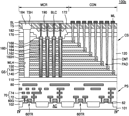
1. An integrated circuit device comprising:
a base structure;
a gate stack on the base structure, wherein the gate stack comprises a plurality of gate electrodes spaced apart from each other in a first direction perpendicular to a main surface of the base structure;
a first upper insulating layer on the gate stack;
a plurality of channel structures that penetrate the gate stack and contact the base structure, wherein each of the plurality of channel structures comprises a respective alignment key that protrudes from the gate stack;
a second upper insulating layer that is in a key opening of the first upper insulating layer and overlaps the respective alignment key of each of the plurality of channel structures;
a top supporting layer on the second upper insulating layer;
a bit line on the top supporting layer; and
a plurality of bit line contacts that penetrate the second upper insulating layer and the top supporting layer and electrically connect respective ones of the plurality of channel structures to the bit line,
wherein a sidewall defining the key opening of the first upper insulating layer comprises a first step.
|