US 12,002,763 B2
Package substrate and semiconductor package including the same
Seungmin Kim, Asan-si (KR)
Assigned to SAMSUNG ELECTRONICS CO., LTD., Suwon-si (KR)
Filed by SAMSUNG ELECTRONICS CO., LTD., Suwon-si (KR)
Filed on Dec. 15, 2022, as Appl. No. 18/081,900.
Application 18/081,900 is a continuation of application No. 17/176,756, filed on Feb. 16, 2021, granted, now 11,552,022.
Claims priority of application No. 10-2020-0079056 (KR), filed on Jun. 29, 2020.
Prior Publication US 2023/0121128 A1, Apr. 20, 2023
This patent is subject to a terminal disclaimer.
Int. Cl. H01L 23/52 (2006.01); H01L 23/48 (2006.01); H01L 23/538 (2006.01); H01L 25/065 (2023.01)
CPC H01L 23/5386 (2013.01) [H01L 23/48 (2013.01); H01L 23/5383 (2013.01); H01L 25/0655 (2013.01)] 20 Claims
OG exemplary drawing
 
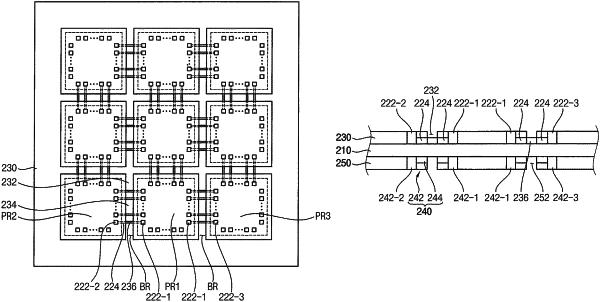
1. A package substrate comprising:
a core insulation;
an upper insulation pattern arranged on the core insulation layer, wherein the upper insulation pattern includes an upper trench;
a lower insulation pattern arranged on the core insulation layer, wherein the lower insulation pattern includes a lower trench; and
a reinforcing portion arranged in at least one of the upper trench or the lower trench.