| CPC H01L 23/5384 (2013.01) [H01L 21/50 (2013.01); H01L 21/76802 (2013.01); H01L 21/76841 (2013.01); H01L 21/76877 (2013.01); H01L 23/3736 (2013.01); H01L 23/5386 (2013.01); H01L 25/0657 (2013.01)] | 20 Claims |
|
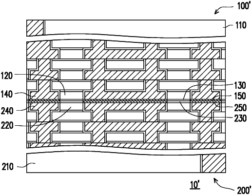
1. A semiconductor device, comprising:
a semiconductor substrate;
an electrical insulating and thermal conductive layer disposed over the semiconductor substrate;
a dielectric structure disposed over the electrical insulating and thermal conductive layer, wherein a thermal conductivity of the electrical insulating and thermal conductive layer is substantially greater than a thermal conductivity of the dielectric structure; and
a circuit layer damascened in the dielectric structure, wherein the circuit layer comprises a bottom surface closest to the semiconductor substrate, and a lower surface of the electrical insulating and thermal conductive layer is substantially coplanar with the bottom surface of the circuit layer.
|