| CPC H01L 23/5226 (2013.01) [H01L 21/76816 (2013.01); H01L 21/76877 (2013.01); H01L 23/5283 (2013.01); H01L 29/66795 (2013.01); H01L 29/785 (2013.01)] | 20 Claims |
|
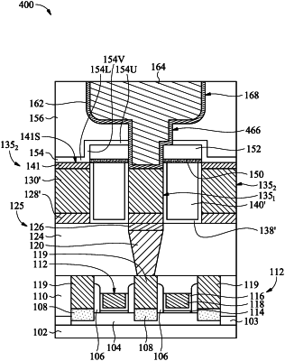
1. An interconnect structure, comprising:
a first metal line and a second metal line surrounded by a first dielectric layer;
wherein the second metal line comprises a glue layer, a metal bulk layer over the glue layer and a metal capping layer over the metal bulk layer;
a dielectric block over a portion of the first dielectric layer between the first metal line and the second metal line;
a second dielectric layer over the dielectric block, the first metal line and the second metal line, wherein a bottom surface of the second dielectric layer is lower than a top surface of the dielectric block;
a first via surrounded by the second dielectric layer and electrically connected to the first metal line;
an encapsulating layer interposing between the first metal line and the first dielectric layer, wherein a top surface of the second metal line is substantially level to a top surface of the encapsulating layer; and
an etching stop layer along and in contact with the top surface of the second metal line and the top surface of the dielectric block, wherein a bottom surface of the etching stop layer is level to the top surface of the encapsulating layer and a top surface of the metal capping layer.
|
|
8. An interconnect structure, comprising:
a first metal line in a first dielectric layer;
a dielectric block over the first dielectric layer;
an etching stop layer over the dielectric block and the first metal line, wherein the etching stop layer includes a first horizontal portion along a top surface of the first metal line, a first vertical portion along a sidewall of the dielectric block, and a second horizontal portion along a top surface of the dielectric block, and a bottom surface of the first horizontal portion of the etching stop layer is lower than a bottom surface of the dielectric block;
a second dielectric layer covering the first horizontal portion and the second horizontal portion of the etching stop layer; and
a catalyst layer between the dielectric block and the first dielectric layer, wherein the bottom surface of the first horizontal portion of the etching stop layer is level to a bottom surface of the catalyst layer.
|
|
14. An interconnect structure, comprising:
a first dielectric layer over a substrate;
a first metal line and a second metal line through the first dielectric layer;
a dielectric block over the first dielectric layer;
an etching stop layer along an upper surface and a sidewall of the dielectric block and an upper surface of the second metal line;
a second dielectric layer over the etching stop layer;
a via extending through the second dielectric layer, the etching stop layer, and the dielectric block to the first metal line; and
a blocking layer between the second metal line and the etching stop layer, wherein the blocking layer includes amphiphilic organic molecules.
|