| CPC H01L 23/5226 (2013.01) [H01L 21/76831 (2013.01); H01L 21/76832 (2013.01)] | 20 Claims |
|
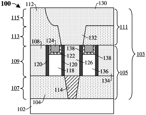
1. An integrated chip, comprising:
a semiconductor substrate;
a dielectric layer disposed over the semiconductor substrate;
a pair of metal lines disposed over an upper surface of the dielectric layer and laterally spaced apart from one another by a cavity, wherein the pair of metal lines have bottom surfaces that are co-planar with the upper surface of the dielectric layer, and a bottom extent of the cavity between the pair of metal lines is defined by the upper surface of the dielectric layer; and
a barrier layer structure extending only along nearest neighboring sidewalls of the pair of metal lines such that lateral extents of the cavity are defined by inner sidewalls of the barrier layer structure.
|