US 12,002,745 B2
High performance integrated RF passives using dual lithography process
Adel A. Elsherbini, Tempe, AZ (US); Mathew J. Manusharow, Phoenix, AZ (US); Krishna Bharath, Phoenix, AZ (US); William J. Lambert, Tempe, AZ (US); Robert L. Sankman, Phoenix, AZ (US); Aleksandar Aleksov, Chandler, AZ (US); Brandon M. Rawlings, Chandler, AZ (US); Feras Eid, Chandler, AZ (US); Javier Soto Gonzalez, Chandler, AZ (US); Meizi Jiao, Chandler, AZ (US); Suddhasattwa Nad, Chandler, AZ (US); and Telesphor Kamgaing, Chandler, AZ (US)
Assigned to Intel Corporation, Santa Clara, CA (US)
Filed by Intel Corporation, Santa Clara, CA (US)
Filed on Dec. 7, 2021, as Appl. No. 17/544,693.
Application 17/544,693 is a division of application No. 15/773,030, granted, now 11,227,825, previously published as PCT/US2015/067157, filed on Dec. 21, 2015.
Prior Publication US 2022/0102261 A1, Mar. 31, 2022
Int. Cl. H05K 1/02 (2006.01); H01F 17/00 (2006.01); H01F 17/06 (2006.01); H01F 27/28 (2006.01); H01F 27/40 (2006.01); H01F 41/04 (2006.01); H01G 4/18 (2006.01); H01G 4/252 (2006.01); H01G 4/30 (2006.01); H01G 4/33 (2006.01); H01L 21/48 (2006.01); H01L 23/498 (2006.01); H01L 23/552 (2006.01); H01L 23/66 (2006.01); H01L 49/02 (2006.01)
CPC H01L 23/49838 (2013.01) [H01F 17/0006 (2013.01); H01F 27/2804 (2013.01); H01F 27/40 (2013.01); H01F 41/041 (2013.01); H01G 4/33 (2013.01); H01L 21/4857 (2013.01); H01L 21/486 (2013.01); H01L 23/49822 (2013.01); H01L 23/49827 (2013.01); H01L 23/66 (2013.01); H01L 28/00 (2013.01); H01L 28/10 (2013.01); H01L 28/60 (2013.01); H01F 2027/2809 (2013.01); H01L 2223/6661 (2013.01)] 5 Claims
OG exemplary drawing
 
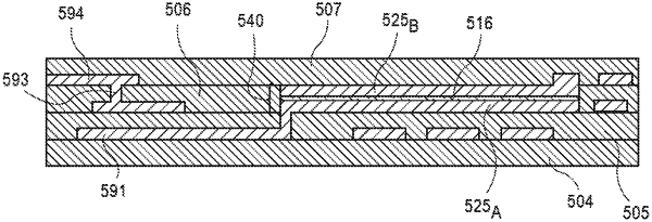
1. A capacitor in an electrical package comprising:
a first dielectric layer;
a first capacitor plate over a top surface of the first dielectric layer and along a sidewall of the first dielectric layer;
a dielectric spacer over a surface of the first capacitor plate;
a second capacitor plate separated from the first capacitor plate by the dielectric spacer layer; and
a second dielectric layer laterally adjacent to the first capacitor plate, the dielectric spacer, and the second capacitor plate, wherein the second dielectric layer has an uppermost surface at a same level as an upper surface of the second capacitor plate.