| CPC H01L 23/49838 (2013.01) [G09G 3/3241 (2013.01); H01L 21/4803 (2013.01); H01L 22/20 (2013.01); H01L 23/4985 (2013.01); H01L 23/544 (2013.01); G09G 2310/0243 (2013.01); G09G 2330/02 (2013.01); H01L 25/18 (2013.01); H10K 59/131 (2023.02)] | 18 Claims |
|
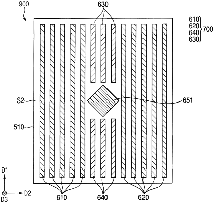
1. A film package comprising:
a base substrate having a bottom surface that includes a first portion and a second portion that are spaced apart from each other in a first direction;
first pad wires disposed on the first portion of the bottom surface of the base substrate and extending in a second direction perpendicular to the first direction;
second pad wires disposed on the second portion of the bottom surface of the base substrate and extending in the second direction;
a light blocking member disposed between the first pad wires and the second pad wires in the first direction;
first dummy patterns disposed on the bottom surface of the base substrate adjacent to and spaced apart from a first side of the light blocking member in the second direction,
the first dummy patterns being disposed between the first pad wires and the second pad wires in the first direction, each of the first dummy patterns extending parallel to the first pad wires and the second pad wires; and
second dummy patterns disposed on the bottom surface of the base substrate adjacent to and spaced apart from a second side of the light blocking member in the second direction, the second dummy patterns being disposed between the first pad wires and the second pad wires in the first direction, each of the second dummy patterns extending parallel to the first pad wires and the second pad wires,
wherein the first and second pad wires are configured for receiving a power supply voltage, and the first and second dummy patterns are not configured for receiving the power supply voltage, wherein the first and second pad wires and the first and second dummy patterns are composed of a similar material as each other.
|