| CPC H01L 23/49811 (2013.01) [H01L 21/4853 (2013.01); H05K 1/0263 (2013.01); H01L 23/053 (2013.01); H01L 24/29 (2013.01); H01L 24/32 (2013.01); H01L 24/48 (2013.01); H01L 24/73 (2013.01); H01L 25/072 (2013.01); H01L 2224/29139 (2013.01); H01L 2224/32225 (2013.01); H01L 2224/48225 (2013.01); H01L 2224/73265 (2013.01)] | 15 Claims |

|
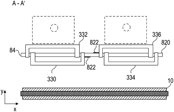
1. A printed circuit board comprises:
a dielectric insulation layer having a top side facing a first side and a bottom side opposite the first side that faces a second side of the dielectric insulation layer;
at least one conducting track formed on the dielectric insulation layer; and
one or more conductor rails, wherein
each of the one or more conductor rails is mechanically coupled to the dielectric insulation layer, and
a first portion of each of the one or more conductor rails is arranged on the first side and a second portion of each of the one or more conductor rails is arranged on the second side of the dielectric insulation layer.
|