| CPC H01L 23/485 (2013.01) [H01L 21/56 (2013.01); H01L 23/3135 (2013.01); H01L 23/13 (2013.01); H01L 23/142 (2013.01); H01L 23/49548 (2013.01); H01L 23/49861 (2013.01)] | 18 Claims |
|
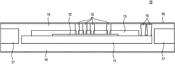
1. A semiconductor device, comprising:
a die carrier;
a semiconductor die disposed on the die carrier, the semiconductor die comprising one or more contact pads;
an encapsulant covering at least partially the semiconductor die and at least a portion of a main face of the die carrier;
an insulation layer covering the encapsulant on an upper main face and on side faces of the encapsulant;
one or more electrical interconnects, each being connected with one of the one or more contact pads of the semiconductor die and extending through the encapsulant; and
a printed circuit board (PCB),
wherein the die carrier is disposed within an opening portion of the PCB,
wherein the insulation layer reaches through a space between side faces of the die carrier and side faces of the PCB to a backside of the die carrier and a backside of the PCB.
|