| CPC H01L 23/481 (2013.01) [H01L 21/566 (2013.01); H01L 23/3157 (2013.01); H01L 23/49811 (2013.01); H01L 23/49827 (2013.01); H01L 24/33 (2013.01); H01L 24/83 (2013.01)] | 7 Claims |
|
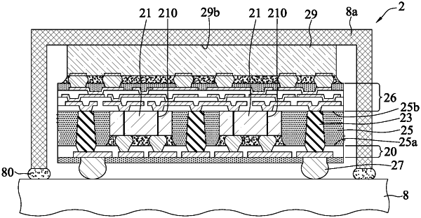
1. An electronic package, comprising:
an encapsulating layer;
at least one interposer board embedded into the encapsulating layer and having a plurality of through-silicon vias;
a plurality of conductive pillars disposed in the encapsulating layer and free from being formed in the at least one interposer board and any interposer board, wherein the plurality of conductive pillars are in direct contact with the encapsulating layer and are free from being in direct contact with the at least one interposer board and the plurality of through-silicon vias, wherein a surface of the encapsulating layer, a surface of the at least one interposer board, end surfaces of the plurality of through-silicon vias and end surfaces of the plurality of conductive pillars are horizontally coplanar; and
at least one semiconductor chip as an electronic component disposed on the encapsulating layer and electrically connected to the plurality of conductive pillars and the plurality of through-silicon vias by a plurality of conductive bumps, wherein the plurality of conductive bumps are in direct contact with the electronic component, the plurality of conductive pillars, and the plurality of through-silicon vias, and the electronic component is free from being embedded in the encapsulating layer.
|