| CPC H01L 23/3735 (2013.01) [H01L 23/367 (2013.01); H01L 23/49816 (2013.01); H01L 23/49822 (2013.01); H01L 23/49833 (2013.01); H01L 23/49838 (2013.01); H01L 24/16 (2013.01); H01L 24/32 (2013.01); H01L 24/73 (2013.01); H01L 25/0655 (2013.01); H01L 25/105 (2013.01); H01L 2224/16227 (2013.01); H01L 2224/16237 (2013.01); H01L 2224/32225 (2013.01); H01L 2224/73204 (2013.01); H01L 2225/1023 (2013.01); H01L 2225/1058 (2013.01); H01L 2225/107 (2013.01); H01L 2225/1094 (2013.01); H01L 2924/1431 (2013.01); H01L 2924/1434 (2013.01); H01L 2924/3511 (2013.01); H01L 2924/3512 (2013.01)] | 18 Claims |
|
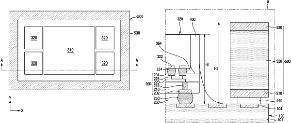
1. A semiconductor package comprising:
a circuit board;
a semiconductor chip on the circuit board;
a stiffener around the semiconductor chip, the stiffener including a first metal layer, a core layer, and a second metal layer sequentially stacked; and
an adhesive layer attaching an upper surface of the circuit board to a bottom surface of the stiffener,
wherein, in a layout view, a first length of at least one of the first metal layer, the core layer, or the second metal layer, extending in a first direction, is longer than a width of the semiconductor chip in the first direction, and
wherein, in a cross-sectional view, a thickness of the core layer is greater than a thickness of at least one of the first metal layer or the second metal layer.
|