| CPC H01L 21/823481 (2013.01) [H01L 21/823412 (2013.01); H01L 21/823431 (2013.01); H01L 21/823437 (2013.01); H01L 29/0665 (2013.01); H01L 29/42392 (2013.01); H01L 29/66439 (2013.01); H01L 29/6653 (2013.01); H01L 29/66545 (2013.01); H01L 29/66553 (2013.01); H01L 29/6656 (2013.01); H01L 29/66795 (2013.01); H01L 29/7851 (2013.01); H01L 29/0673 (2013.01); H01L 29/775 (2013.01); H01L 29/78696 (2013.01)] | 20 Claims |
|
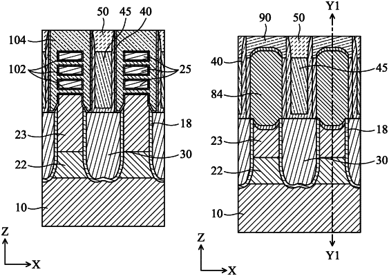
9. A method of manufacturing a semiconductor device, comprising:
forming fin structures each including a stacked layer of first semiconductor layers and second semiconductor layers disposed over a bottom fin structure and a hard mask layer over the stacked layer;
forming an isolation insulating layer so that the hard mask layer and the stacked layer are exposed from the isolation insulating layer;
forming a sacrificial cladding layer over the exposed hard mask layer and stacked layer;
performing an etching operation to remove lateral portions of the sacrificial cladding layer, thereby leaving the sacrificial cladding layer on sidewalls of the exposed hard mask layer and stacked layer, wherein during the etching operation, a protection layer is formed over the sacrificial cladding layer;
forming a wall fin structure between the fin structures;
removing the hard mask layer;
forming a sacrificial gate structure over the fin structures;
forming sidewall spacers on sidewalls of the sacrificial gate structure and sidewalls of a part of the wall fin structure;
forming a source/drain structure over the fin structures adjacent the sidewall spacers;
forming a dielectric layer over the source/drain structure;
removing the sacrificial gate structure;
removing the sacrificial cladding layer;
removing the first semiconductor layers; and
forming a metal gate structure around the second semiconductor layers.
|