| CPC H01L 21/67265 (2013.01) [G06T 7/13 (2017.01); H01L 21/6732 (2013.01); H01L 21/67778 (2013.01)] | 25 Claims |
|
1. A semiconductor wafer mapping apparatus comprising:
a frame forming a wafer load opening communicating with a load station for a substrate carrier disposed to hold more than one wafers vertically distributed in the substrate carrier for loading through the wafer load opening;
a movable arm movably mounted to the frame so as to move relative to the wafer load opening and having at least one end effector movably mounted to the movable arm to load wafers from the substrate carrier through the wafer load opening;
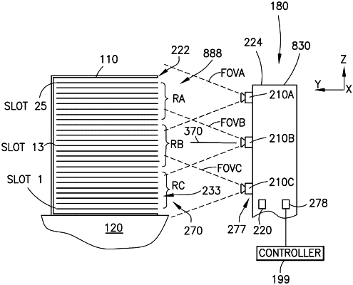
an image acquisition system including an array of cameras arranged on a common support and each camera is fixed with respect to the common support that is static with respect to each camera of the array of cameras, wherein each respective camera is positioned with a field of view disposed to view, through the wafer load opening with the common support positioned by the movable arm at a common position, a different separate part of the substrate carrier with wafer slots for holding at least one of the more than one wafers, separate and different from parts of the substrate carrier with different wafer slots for holding wafers different than the at least one wafer viewed by each other camera with the common support at the common position, and each wafer held in the substrate carrier is imaged by the array of cameras with the common support at the common position; and
an illumination source connected to the common support configured so as to illuminate, through the wafer load opening with the common support in the common position, an outer edge of each wafer in the substrate carrier, which edge delineates upper and lower edge boundaries of the outer edge of the wafer, the illumination source being disposed with respect to each camera so that the outer edge directs reflected edge illumination, from the illumination source, at each camera, and optically blanks, at the upper and lower edge boundaries, background reflection light, viewed by each camera through the wafer load opening with the common support at the common position;
wherein the outer edge of the wafer is defined in the image with the upper and lower edge boundaries in relief in image contrast, formed by and between the edge reflection and the optically blanked background, registered by each camera so as to effect edge detection of each wafer in the substrate carrier with the common support at the common position.
|