| CPC H01L 21/67069 (2013.01) [H01L 21/67253 (2013.01); H10B 12/03 (2023.02)] | 16 Claims |
|
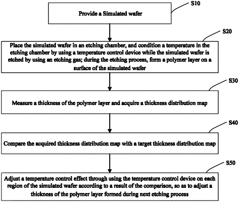
1. A semiconductor equipment regulation method, comprising:
providing a simulated wafer;
placing the simulated wafer in an etching chamber, and conditioning a temperature in the etching chamber by using a temperature control device while performing an etching process on the simulated wafer by using an etching gas; during the etching process, a polymer layer is formed on a surface of the simulated wafer;
measuring a thickness of the polymer layer and acquiring a thickness distribution map;
comparing the acquired thickness distribution map with a target thickness distribution map; and
adjusting a temperature control effect through using the temperature control device on each region of the simulated wafer according to a result of the comparison, so as to adjust a thickness of the polymer layer formed during a next etching process.
|