| CPC H01L 21/50 (2013.01) [H01L 23/16 (2013.01); H01L 25/0657 (2013.01); H01L 21/603 (2021.08); H01L 23/295 (2013.01); H01L 23/3142 (2013.01); H01L 25/50 (2013.01)] | 11 Claims |
|
1. A semiconductor device, comprising:
a substrate;
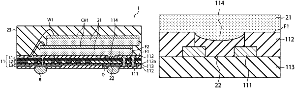
a first resin layer provided above a first surface of the substrate, the first resin layer including a plurality of types of resins having different molecular weights and a filler;
a first semiconductor chip provided above the first resin layer and the first surface; and
a second resin layer provided in at least a part of a first region between the substrate and the first resin layer, the second resin layer directly contacting the first resin layer, the second resin layer including:
at least one type of resins among the plurality of types of resins having a molecular weight smaller than a molecular weight of other types of resins among the plurality of types of resins, and
a filler having a lower concentration than the filler of the first resin layer,
a third resin layer covering the first resin layer, the second resin layer and the substrate,
wherein
the third resin layer directly contacting the first surface of the substrate,
the first semiconductor chip directly contacting the first resin layer,
the substrate includes a recess, and the second resin layer is disposed in a second region between the recess and the first resin layer,
the recess has a first metal film and a second metal film, and the first and second metals are physically separated in the recess,
a first part of the first metal film and a first part of the second metal film directly contacting a bottom surface of the recess,
a second part of the first metal film and a second part of the second metal film being embedded in a side wall of the recess.
|