| CPC H01L 21/3212 (2013.01) [B24B 37/044 (2013.01); B24B 37/107 (2013.01); C09G 1/02 (2013.01)] | 20 Claims |
|
1. A method for chemical-mechanical polishing (CMP), comprising:
receiving a metal layer stack in a dielectric structure, wherein the metal layer stack comprises at least a first metal layer and a second metal layer over the first metal layer, and a top surface of the first metal layer and a top surface of the second metal layer being exposed;
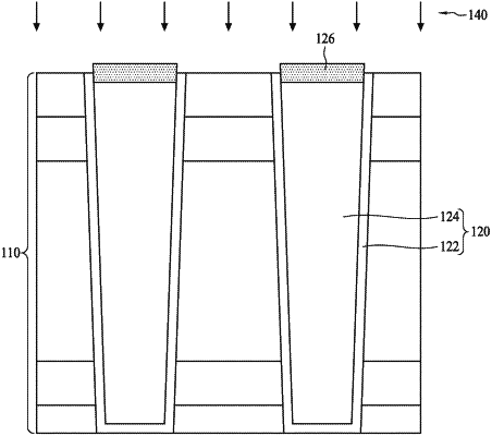
forming a protecting layer over the top surface of the second metal layer;
etching a portion of the first metal layer, wherein the protecting layer protects the second metal layer during the etching of the portion of the first metal layer, and a top surface of the etched first metal layer is lower than a top surface of the protecting layer;
removing the protecting layer from the second metal layer; and
removing a portion of the first metal layer, a portion of the second metal layer and a portion of the dielectric structure, wherein a top surface of the first metal layer, a top surface of the second metal layer and a top surface of the dielectric structure form a flush surface.
|
|
8. A method for chemical-mechanical polishing (CMP), comprising:
forming a first metal layer in a dielectric structure and a second metal layer covering the first metal layer;
removing a portion of the second metal layer to expose the first metal layer;
forming a protecting layer over the second metal layer and etching the first metal layer, wherein a top surface of the etched first metal layer is lower than a top surface of the protecting layer;
removing the protecting layer to expose the second metal layer; and
removing a portion of the first metal layer, a portion of the second metal layer and a portion of the dielectric structure, wherein a top surface of the first metal layer, a top surface of the second metal layer and a top surface of the dielectric structure form a flush surface.
|