| CPC H01L 21/3086 (2013.01) [H01L 21/0332 (2013.01); H01L 21/0337 (2013.01); H01L 21/0338 (2013.01); H01L 21/3081 (2013.01); H01L 21/3088 (2013.01); H01L 21/31144 (2013.01); H01L 21/32139 (2013.01); H01L 21/76816 (2013.01)] | 10 Claims |
|
1. A Tip-to-Tip pattern preparation method, comprising:
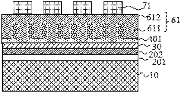
step S1: providing a substrate, and sequentially forming a layer to be etched, a first hard mask layer, a second hard mask layer, a sacrificial layer, a first dielectric layer and a first photoresist layer on the substrate, performing EUV lithography on the first photoresist layer to form a first patterned photoresist layer, which has a first Tip-to-Tip pattern;
step S2: using the first patterned photoresist layer as a mask, sequentially etching the first dielectric layer and the sacrificial layer to the upper surface of the second hard mask layer, thus forming a patterned sacrificial layer which has the first Tip-to-Tip pattern;
step S3: forming a spacer layer on the sidewall of the patterned sacrificial layer to fill Tip-to-Tip spaces of the first Tip-to-Tip pattern and expose a part of the upper surface of the second hard mask layer in other area;
step S4: forming a patterned protective layer to mask areas exposed by the patterned sacrificial layer and the spacer layer and expose the upper surface of the patterned sacrificial layer, using the patterned protective layer as a mask to remove the patterned sacrificial layer and the second hard mask layer thereunder, thus exposing a part of the upper surface of the first hard mask layer;
step S5: removing the patterned protective layer and sequentially forming a second dielectric layer and a second photoresist layer above the first hard mask layer, the second hard mask layer, and the spacer layer, and performing the EUV lithography on the second photoresist layer to form a second patterned photoresist layer, which has a second Tip-to-Tip pattern, the second Tip-to-Tip pattern and the first Tip-to-Tip pattern are interlaced;
step S6: using the second patterned photoresist layer as a mask, sequentially etching the second dielectric layer, the spacer layer and the second hard mask layer to the upper surface of the first hard mask layer, thus transferring the second Tip-to-Tip pattern into the spacer layer and the second hard mask layer;
step S7: removing the second patterned photoresist layer and the second dielectric layer, using the spacer layer and the second hard mask layer as a mask and etching the first hard mask layer and the layer to be etched to the upper surface of the substrate, thus forming a Tip-to-Tip pattern composed of the first Tip-to-Tip pattern interlaced with the second Tip-to-Tip pattern in the layer to be etched.
|