| CPC H01J 37/32183 (2013.01) [H01J 37/32119 (2013.01); H01J 37/32697 (2013.01); H01J 37/32715 (2013.01); H01J 37/32899 (2013.01); H01J 2237/3321 (2013.01); H01J 2237/334 (2013.01)] | 13 Claims |
|
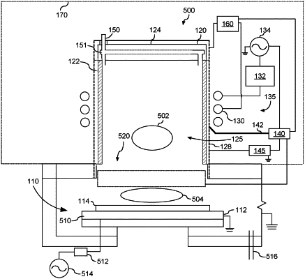
1. A plasma processing apparatus, comprising:
a plasma chamber configured to be able to hold a plasma;
a dielectric window forming at least a portion of a wall of the plasma chamber;
a gas supply configured supply a process gas to the plasma chamber;
an inductive coupling element located proximate the dielectric window, the inductive coupling element configured to generate a plasma from the process gas in the plasma chamber when energized with radio frequency (RF) energy;
a processing chamber having a workpiece support configured to support a workpiece, the processing chamber being in fluid communication with the plasma chamber;
an electrostatic shield located between the inductive coupling element and the dielectric window, the electrostatic shield having a stray capacitance to the inductive coupling element;
a tunable reactive impedance circuit coupled between the inductive coupling element and the electrostatic shield, the tunable reactive impedance circuit configured to adjust a reactance between the inductive coupling element and the electrostatic shield between a condition of capacitive reactance and a condition of inductive reactance at a frequency of RF energy supplied to the inductive coupling element;
wherein the tunable reactive impedance circuit is operable to achieve an inductive reactance at least approximately equal to the capacitive reactance of the stray capacitance;
a voltage sensor, the voltage sensor configured to measure a voltage of the electrostatic shield; and
a controller coupled to the tunable reactive impedance circuit and a RF power generator, the controller configured to control the tunable reactive impedance circuit and the RF power generator based on a measured voltage of the electrostatic shield.
|