| CPC H01J 37/32174 (2013.01) [H01J 37/32128 (2013.01); H01J 37/32146 (2013.01); H01J 37/32091 (2013.01); H01J 37/32577 (2013.01)] | 20 Claims |
|
1. A wafer processing apparatus comprising:
a chamber configured to load a wafer;
a radio frequency (RF) power source configured to generate plasma ions in the chamber; and
a voltage waveform generator configured to accelerate the plasma ions toward the wafer,
wherein the voltage waveform generator comprises:
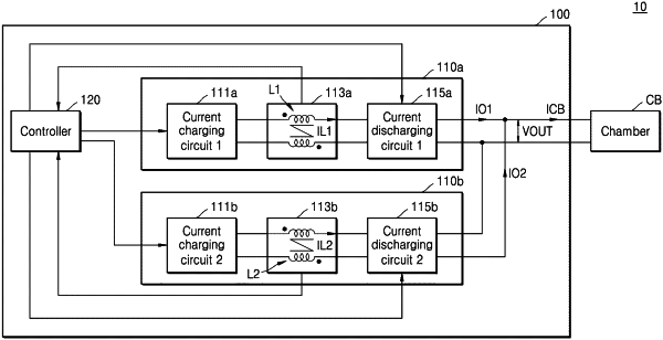
a pulse circuit comprising a first inductive element configured to store a first internal current, the pulse circuit being configured to apply a pulse voltage to the chamber by adjusting a chamber current applied to the chamber; and
a slope circuit configured to generate a slope in an on-duty of the pulse voltage,
wherein the pulse circuit and the slope circuit are electrically connected in parallel to an input terminal of the chamber, and
wherein the pulse circuit comprises a first current discharging circuit comprising:
a first switch, a first diode, a second switch and a second diode arranged in series in a first path configured to allow the first internal current to enter a first terminal of the chamber, and
a third switch, a third diode, a fourth switch and a fourth diode arranged in series in a second path configured to allow the first internal current to enter a second terminal of the chamber opposite to the first terminal.
|