| CPC H01G 4/30 (2013.01) [H01G 4/012 (2013.01); H01G 4/12 (2013.01); H01G 4/224 (2013.01); H01G 4/232 (2013.01)] | 20 Claims |
|
1. A multilayer electronic component comprising:
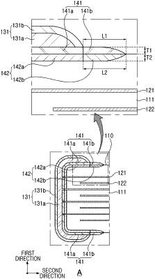
a body including a plurality of dielectric layers and a plurality of internal electrodes alternately disposed with the dielectric layer interposed therebetween in a first direction and including first and second surfaces opposing each other in the first direction, third and fourth surfaces connected to the first and second surfaces and opposing each other in a second direction, and fifth and sixth surfaces connected to the first to fourth surfaces and opposing each other in a third direction;
external electrodes disposed on external surfaces of the body and connected to the internal electrodes; and
sealing portions disposed on outer surfaces of the body,
wherein the external electrodes and the sealing portions include glass,
the sealing portions include first sealing portions that are disposed between the body and the external electrodes, and second sealing portions that extend from the first sealing portions in the second direction and are not in contact with the external electrodes, and
an average length of the second sealing portions is 20 μm or more.
|