| CPC H01G 4/30 (2013.01) [H01G 4/012 (2013.01); H01G 4/12 (2013.01); H01G 4/248 (2013.01); H05K 1/181 (2013.01); H05K 2201/10015 (2013.01)] | 7 Claims |
|
1. A method of producing a multi-layer ceramic electronic component, comprising:
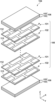
forming an internal electrode pattern having a predetermined thickness on each unsintered ceramic sheet of a plurality of unsintered ceramic sheets, each unsintered ceramic sheet comprising an electrode non-formation region where the internal electrode pattern is absent;
forming a dielectric pattern on each unsintered ceramic sheet of the plurality of unsintered ceramic sheets having the internal electrode pattern fowled thereon, the dielectric pattern being formed only in the respective electrode non-formation region of each unsintered ceramic sheet such that the dielectric pattern occupies 75% or more and less than 100% of the electrode non-formation region;
laminating in a first direction the plurality of unsintered ceramic sheets, the internal electrode pattern and the dielectric pattern being formed on each unsintered ceramic sheet of the plurality of unsintered ceramic sheets, and thereby forming an unsintered multi-layer body;
cutting the unsintered multi-layer body, thereby forming an unsintered ceramic body including a plurality of internal electrodes laminated in the first direction;
sintering the unsintered ceramic body to form a sintered ceramic body; and
forming a pair of external electrodes that are connected to the plurality of internal electrodes and face each other in a second direction orthogonal to the first direction,
a dimension of the sintered ceramic body in the first direction being 1.1 times or more and 1.6 times or less a dimension of the sintered ceramic body in a third direction orthogonal to the first direction and the second direction,
wherein the internal electrode pattern on each unsintered ceramic sheet of the plurality of unsintered ceramic sheets comprises a first column of internal electrodes and a second column of internal electrodes that are displaced, in the second direction, by one chip compared to the internal electrodes in the first column.
|