| CPC H01F 27/2804 (2013.01) [H01F 17/0013 (2013.01); H01F 27/24 (2013.01); H01F 27/2847 (2013.01); H01F 41/041 (2013.01); H01F 41/042 (2013.01); H01F 41/046 (2013.01); H01F 17/0033 (2013.01); H05K 1/181 (2013.01); H05K 1/185 (2013.01); H05K 2201/1003 (2013.01)] | 17 Claims |
|
1. A component carrier, comprising:
a stack comprising at least one electrically conductive layer structure and at least one electrically insulating layer structure;
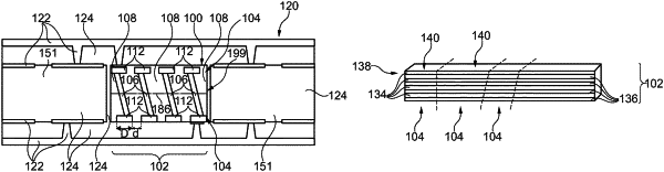
an inductor embedded in or surface mounted on the stack, the inductor having a plurality of stacked layer structures made of component carrier material and electrically conductive plate structures; and
a plurality of electrically conductive interconnect structures connecting the electrically conductive plate structures to thereby form an inductance with multiple windings, wherein a stacking direction of the stack is slanted or perpendicular to a stacking direction of the stacked layer structures.
|