| CPC H01B 5/14 (2013.01) [B05D 1/26 (2013.01); B05D 3/0254 (2013.01); B05D 3/06 (2013.01); B05D 3/067 (2013.01); B05D 3/142 (2013.01); B05D 7/54 (2013.01); G02B 1/11 (2013.01); G02B 1/14 (2015.01)] | 12 Claims |
|
1. An optically consistent transparent conductive film, wherein the optically consistent transparent conductive film comprises a substrate, an optically consistent conductive layer and a protective layer;
wherein the substrate comprises a rigid or/and flexible substrate;
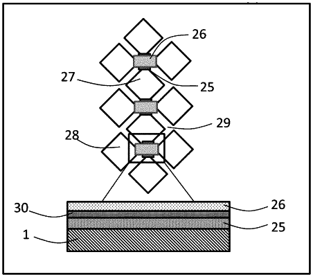
the optically consistent conductive layer comprises a conductive area, the conductive area comprises metal nanowires A and nanoparticles B, the metal nanowires A superimpose or crosslink to form a network in a conductive area, the nanoparticles B function to weld the metal nanowires A; the nanoparticles B are uniformly distributed in the conductive area, the influence of the nanoparticles B on the conductivity of the metal nanowires A is less than 50%; the optically consistent conductive layer comprises a non-conductive area obtained by etching the metal nanowires A in the conductive area, the non-conductive area comprises uniformly distributed nanoparticles B, the nanoparticles B do not form a continuous conductive pathway with each other in the non-conductive area; the vaporization temperature of the nanoparticles B is higher than that of the metal nanowires A; the corrosion rate of the metal nanowires A is faster than nanoparticles B; and the refractive index of the nanoparticles B is adapted to that of the metal nanowires A; and
the protective layer is coated on the surface of the optically consistent conductive layer, and the surface resistance value is not changed; the protective layer contains dendrimers having a chelating effect, the dendrimer has an effect of trapping metal ions to form a chelate to inhibit migration of metal ions; the protective layer further comprises dispersed nanoparticles B, and the nanoparticles B have the effect of reducing the chromaticity of the conductive area.
|