| CPC G11C 7/222 (2013.01) [G11C 7/1048 (2013.01); G11C 7/1057 (2013.01); G11C 7/1084 (2013.01)] | 20 Claims |
|
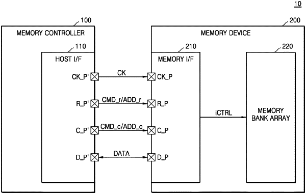
1. A memory device comprising:
a clock pin configured to receive a clock signal;
row pins configured to receive a first active command and a first precharge command during a first time period, and receive a second active command and a second precharge command during a second time period; and
column pins configured to receive a first read command or a first write command during the first time period, and receive a second read command or a second write command during the second time period,
wherein during the first time period, the row pins are configured to receive the first active command during a first sub-period and receive the first precharge command during a second sub-period corresponding to a rising edge of the clock signal after receiving the first active command, and the column pins are configured to receive the first read command or the first write command during a third sub-period,
wherein during the second time period, the row pins are configured to receive the second active command during a fourth sub-period and receive the second precharge command during a fifth sub-period corresponding to a falling edge of the clock signal after receiving the second active command, and the column pins are configured to receive the second read command or the second write command during a sixth sub-period,
wherein a length of each of the first sub-period and the fourth sub-period is one and a half (1.5) cycles of the clock signal, a length of each of the second sub-period and the fifth sub-period is a half (0.5) cycle of the clock signal, and a length each of the third sub-period and the sixth sub-period is one (1) cycle of the clock signal.
|