| CPC G11C 7/22 (2013.01) [G11C 5/063 (2013.01); G11C 11/4063 (2013.01); G11C 29/02 (2013.01); G11C 29/022 (2013.01); G11C 29/025 (2013.01); G11C 29/028 (2013.01); G11C 5/025 (2013.01); G11C 5/04 (2013.01); G11C 5/06 (2013.01); G11C 7/18 (2013.01); G11C 11/4097 (2013.01)] | 20 Claims |
|
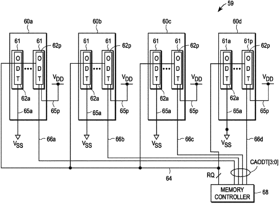
1. A memory controller to control the operation of a memory device, the memory controller comprising:
a command/address (CA) transmission circuit;
the memory controller to:
send, using the CA transmission circuit, command/address (CA) signals via a CA bus to respective inputs of the memory device and a chip select signal to a chip select input of the memory device; and
send to the memory device:
register values, for storage in a plurality of registers of the memory device, including a register value that selects from two or more impedance values of on-die termination (ODT) impedances to apply to each of the respective inputs of the memory device that receive the CA signals;
wherein the register values include one or more register values to selectively enable application of the ODT impedances to the respective inputs that receive the CA signals, and a register value that selectively enables application of a CS ODT impedance to the chip select input.
|