| CPC G11C 19/184 (2013.01) [G09G 3/3648 (2013.01); G09G 3/3677 (2013.01); G09G 3/3266 (2013.01); G09G 2300/0426 (2013.01); G09G 2310/0267 (2013.01); G09G 2310/0275 (2013.01); G09G 2310/0286 (2013.01); G09G 2310/0289 (2013.01); G09G 2320/02 (2013.01); G09G 2320/043 (2013.01); G09G 2330/021 (2013.01); G09G 2330/023 (2013.01)] | 4 Claims |
|
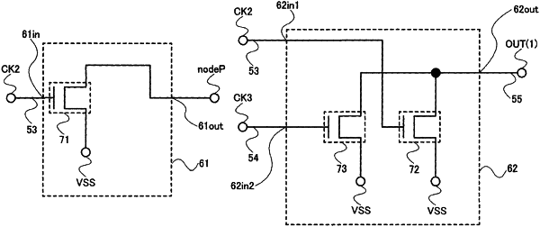
1. A display device comprising:
a gate driver comprising a first transistor, a second transistor, a third transistor, a fourth transistor, a fifth transistor, a sixth transistor, and a seventh transistor; and
a pixel comprising an eighth transistor,
wherein one of a source and a drain of the first transistor is electrically connected to a gate signal line,
wherein the other of the source and the drain of the first transistor is electrically connected to a clock signal line,
wherein a gate of the first transistor is electrically connected to one of a source and a drain of the third transistor,
wherein one of a source and a drain of the second transistor is electrically connected to the gate signal line,
wherein the other of the source and the drain of the second transistor is electrically connected to a first power source line,
wherein a gate of the second transistor is electrically connected to a gate of the fourth transistor,
wherein the other of the source and the drain of the third transistor is electrically connected to a second power source line,
wherein a gate of the third transistor is electrically connected to a first wiring to which a start pulse is input,
wherein one of a source and a drain of the fourth transistor is electrically connected to the gate of the first transistor,
wherein the other of the source and the drain of the fourth transistor is electrically connected to a third power source line,
wherein one of a source and a drain of the fifth transistor is electrically connected to the gate of the first transistor,
wherein the other of the source and the drain of the fifth transistor is electrically connected to the third power source line,
wherein a gate of the fifth transistor is electrically connected to one of a source and a drain of the sixth transistor,
wherein the other of the source and the drain of the sixth transistor is electrically connected to a second wiring,
wherein a gate of the sixth transistor is electrically connected to one of a source and a drain of the seventh transistor,
wherein the other of the source and the drain of the seventh transistor is electrically connected to the third power source line,
wherein a gate of the seventh transistor is electrically connected to the gate of the first transistor, and
wherein a gate of the eighth transistor is electrically connected to the gate signal line.
|