US 12,002,520 B2
Voltage generation circuit which is capable of executing high-speed boost operation
Tatsuro Midorikawa, Kamakura (JP); and Masami Masuda, Chigasaki (JP)
Assigned to KIOXIA CORPORATION, Tokyo (JP)
Filed by KIOXIA CORPORATION, Tokyo (JP)
Filed on Jul. 10, 2023, as Appl. No. 18/349,443.
Application 18/349,443 is a continuation of application No. 17/647,509, filed on Jan. 10, 2022, granted, now 11,742,033.
Application 17/647,509 is a continuation of application No. 17/031,656, filed on Sep. 24, 2020, granted, now 11,250,919, issued on Feb. 15, 2022.
Application 17/031,656 is a continuation of application No. 16/670,862, filed on Oct. 31, 2019, granted, now 10,818,364, issued on Oct. 27, 2020.
Application 16/670,862 is a continuation of application No. 16/273,979, filed on Feb. 12, 2019, granted, now 10,515,706, issued on Dec. 24, 2019.
Application 16/273,979 is a continuation of application No. 15/417,489, filed on Jan. 27, 2017, granted, now 10,242,748, issued on Mar. 26, 2019.
Application 15/417,489 is a continuation of application No. 14/257,501, filed on Apr. 21, 2014, granted, now 9,589,656, issued on Mar. 7, 2017.
Application 14/257,501 is a continuation of application No. 13/235,437, filed on Sep. 18, 2011, granted, now 8,755,235, issued on Jun. 17, 2014.
Claims priority of application No. 2010-245285 (JP), filed on Nov. 1, 2010.
Prior Publication US 2023/0352103 A1, Nov. 2, 2023
Int. Cl. G11C 16/30 (2006.01); H02M 3/07 (2006.01)
CPC G11C 16/30 (2013.01) [H02M 3/07 (2013.01)] 9 Claims
OG exemplary drawing
 
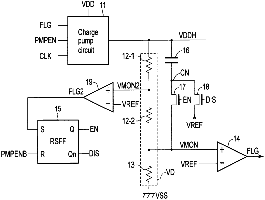
1. A voltage generation circuit comprising:
a charge pump circuit configured to output a first voltage;
a first voltage division circuit configured to divide the first voltage to a second voltage;
a second voltage division circuit configured to divide a difference between the first voltage and the second voltage to a third voltage
a first amplifier having a first input terminal and a second input terminal, the first amplifier configured to input the second voltage from the first input terminal and to input a fourth voltage from the second input terminal, the first amplifier configured to output a signal which controls the charge pump circuit;
a second amplifier having a third input terminal and a fourth input terminal, the second amplifier configured to input the third voltage from the third input terminal and to input the fourth voltage from the fourth input terminal, the second amplifier configured to output a signal which controls a part of the voltage generation circuit;
a capacitor having a first end connected to an output terminal of the charge pump circuit and a second end connected to the first input terminal of the first amplifier via a first transistor.