| CPC G11C 16/24 (2013.01) [G11C 16/0483 (2013.01); G11C 16/26 (2013.01)] | 20 Claims |
|
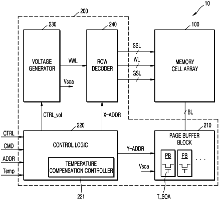
1. A memory device comprising:
a memory cell array including a plurality of memory cells;
a page buffer circuit connected to the memory cell array through a plurality of bit lines and comprising a page buffer connected to each of the plurality of bit lines, the page buffer comprising at least one first latch for storing data based on a voltage level of a first sensing node; and
a control circuit configured to adjust a level of a voltage signal provided to the page buffer circuit,
wherein the page buffer further comprises a trip control transistor arranged between the at least one first latch and the first sensing node, and
wherein the control circuit is further configured to, based on a read operation being performed on the memory cell array, control a trip control voltage to be provided to a gate of the trip control transistor, and control a level of the trip control voltage to vary according to a temperature of the memory device.
|