| CPC G11C 16/24 (2013.01) [G11C 16/10 (2013.01); G11C 16/14 (2013.01)] | 14 Claims |
|
1. A semiconductor memory device comprising:
a memory cell array including a plurality of memory cells for storing data;
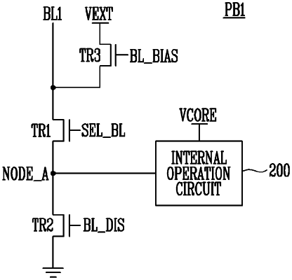
a page buffer coupled to at least one memory cell among the plurality of memory cells through a bit line and configured to store data in the at least one memory cell; and
control logic configured to control an operation of the page buffer,
wherein the page buffer comprises:
a first transistor coupled between the bit line and a first node;
a second transistor coupled between the bit line and an external power voltage terminal; and
an internal operation circuit coupled to the first node,
wherein the control logic is configured to:
control, when a program inhibit bias is transmitted to the bit line, the page buffer to transmit the program inhibit bias from the internal operation circuit to the bit line by turning on the first transistor and disconnect between the external power voltage terminal and the bit line by turning off the second transistor; and
apply, to suppress occurrence of a leakage current from a side of the bit line to a side of the second transistor, a first voltage greater than 0V to the external power voltage terminal while the program inhibit bias is transmitted to the bit line during a program operation.
|