| CPC G11C 16/0483 (2013.01) [G11C 16/08 (2013.01)] | 20 Claims |
|
1. A semiconductor device comprising:
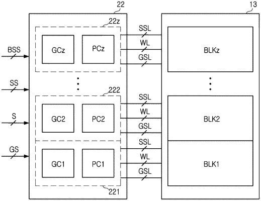
a memory cell array including a plurality of memory blocks, each of the plurality of memory blocks including select transistors and memory cells;
an address decoder configured to generate a first control signal and a second control signal in response to a received address;
a plurality of metal lines connected to the plurality of memory blocks;
pass transistors configured to electrically connect metal lines, connected to a selected memory block, among the plurality of metal lines, to the address decoder in response to the first control signal; and
ground transistors configured to supply a first voltage to metal lines, connected to unselected memory blocks, among the plurality of metal lines, in response to the second control signal, wherein:
the ground transistors include at least one common gate structure, at least one common active region, and individual active regions, and each of at least one the common gate structure and the at least one common active region are shared by two or more ground transistors, among the ground transistors; and
each of at least one the common gate structure is between and contacting one of the at least one common active region and at least two of the individual active regions and includes a first region extending in a first direction and a second region extending in a second direction, intersecting the first direction.
|