| CPC G11C 16/0483 (2013.01) [H10B 41/10 (2023.02); H10B 41/20 (2023.02); H10B 41/27 (2023.02); H10B 41/35 (2023.02); H10B 41/41 (2023.02); H10B 43/10 (2023.02); H10B 43/20 (2023.02); H10B 43/27 (2023.02); H10B 43/35 (2023.02); H10B 43/40 (2023.02)] | 20 Claims |
|
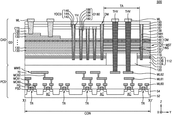
1. A semiconductor device comprising:
a peripheral circuit structure;
a substrate on the peripheral circuit structure;
a pair of word line cut structures extending longitudinally in a first horizontal direction on the substrate, the pair of word line cut structures being spaced apart from each other in a second horizontal direction that is perpendicular to the first horizontal direction; and
a memory cell block that is between the pair of word line cut structures and on the substrate,
wherein the memory cell block comprises:
a memory stack structure including a plurality of gate lines overlapping each other in a vertical direction;
an interlayer insulation layer on an edge portion of each of the plurality of gate lines;
a dam structure extending through the memory stack structure and the interlayer insulation layer;
an intersection direction cut structure extending through the memory stack structure and the interlayer insulation layer in the vertical direction and extending longitudinally in a horizontal direction that traverses the first horizontal direction, the intersection direction cut structure being spaced apart from the dam structure in the first horizontal direction; and
a plurality of dummy channel structures between the intersection direction cut structure and the dam structure.
|