| CPC G09G 3/3275 (2013.01) [G09G 3/2003 (2013.01); H10K 59/124 (2023.02); H10K 59/131 (2023.02); H10K 59/353 (2023.02); G09G 2300/0426 (2013.01); G09G 2300/0452 (2013.01)] | 21 Claims |
|
1. A display panel comprising:
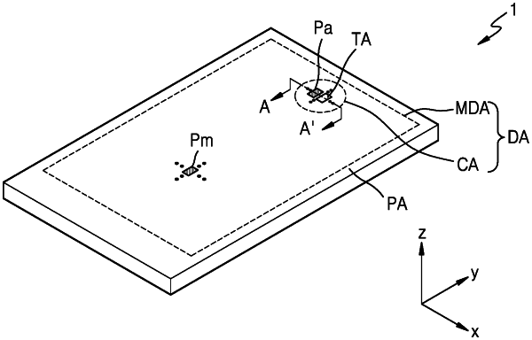
a 1-1st sub-pixel and a 1-2nd sub-pixel disposed over a substrate to be in a main display area, the main display area outside a component area in a plan view;
a 2-1st sub-pixel and a 2-2nd sub-pixel disposed over the substrate to be in the component area, the 2-1st sub-pixel and the 2-2nd sub-pixel including thin-film transistors, each of the thin-film transistors having a semiconductor layer; and
a conductive layer disposed between the semiconductor layer and the substrate, the conductive layer including an opening having a polygonal shape in the component area in the plan view, at least one internal angle of the opening being an obtuse angle.
|