| CPC G09G 3/3233 (2013.01) [G09G 2300/0421 (2013.01); G09G 2300/0819 (2013.01); G09G 2320/0252 (2013.01); H10K 59/1216 (2023.02)] | 20 Claims |
|
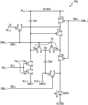
1. An organic light-emitting display apparatus comprising:
a substrate extending in a first direction and a second direction;
a first scan line, a second scan line, and a third scan line configured to respectively transfer a first scan signal, a second scan signal, and a third scan signal, the first-to-third scan lines extending in the first direction;
a data line configured to transfer a data voltage and extending in the second direction;
a power line configured to transfer a driving voltage;
a first voltage line and a second voltage line configured to respectively transfer a first initialization voltage and a second initialization voltage and extending in the first direction; and
a plurality of pixels provided on the substrate in the first direction and the second direction,
wherein:
each of the plurality of pixels comprises:
a light-emitting device;
a driving thin film transistor (TFT) for controlling a magnitude of a current flowing from the power line to the light-emitting device according to a gate-source voltage;
a storage capacitor disposed between the power line and a gate of the driving TFT;
a scan TFT configured to transfer the data voltage to a source of the driving TFT in response to the first scan signal;
a first compensation TFT and a second compensation TFT connected to each other in series to connect a drain of the driving TFT to the gate of the driving TFT in response to the first scan signal;
a gate initialization TFT configured to apply the first initialization voltage to the gate of the driving TFT in response to the second scan signal; and
an anode initialization TFT configured to apply the second initialization voltage to an anode of the light-emitting device in response to the third scan signal; and
on a pixel row composed of pixels on a same row among the plurality of pixels, the second voltage line is disposed between the first voltage line and the first scan line in the second direction in a plan view.
|