| CPC G09G 3/3208 (2013.01) [G09G 2300/0819 (2013.01); G09G 2310/0291 (2013.01); G09G 2320/0223 (2013.01); G09G 2330/021 (2013.01)] | 5 Claims |
|
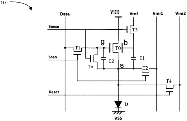
1. A driving method for driving a compensation circuit, the compensation circuit comprising:
a dual-gate transistor, having a first gate electrically connected to a first node, a second gate electrically connected to a second node, a source electrically connected to a first power supply terminal, and a drain electrically connected to a third node;
a light emitting device, electrically connected between the third node and a second power supply terminal;
a first transistor, having a gate receiving a first control signal, a source receiving a data signal, and a drain electrically connected to the first node;
a second transistor, having a gate receiving the first control signal, a source receiving a writing signal, and a drain electrically connected to the third node;
a third transistor, having a gate receiving a second control signal, a source of receiving a first reset signal, and a drain electrically connected to the second node
a fourth transistor, having a gate receiving a third control signal, a source receiving a second reset signal, and a drain electrically connected to the third node;
a fifth transistor, having a gate receiving the second control signal, a source electrically connected to the first node, and a drain electrically connected to the third node;
a first capacitor, connected between the second node and the third node; and
a second capacitor, connected between the first node and the third node;
wherein the driving method comprises:
in a first reset stage, turning on the fourth transistor in response to the third control signal such that the second reset signal is output to the third node to reset the light-emitting device, and turning off the third transistor and the fifth transistor in response to the second control signal;
in a second reset stage, turning on the third transistor and the fifth transistor in response to the second control signal such that the first reset signal is output to the second node and the first reset signal is output to the second node to maintain the voltage level of the first node to be identical to the voltage level of the third node, and turning on the fourth transistor in response to the third control signal such that and the second reset signal continues to be output to the third node;
in a compensation stage, turning on the third transistor in response to the second control signal such that the first reset signal continues to be output to the second node, turning off the fourth transistor in response to the third control signal, turning on the fifth transistor in response to the second control signal to maintain the voltage level of the first node to be identical to the voltage level of the third node, and utilizing a first power supply terminal to charge the third node until a voltage difference between the second node and the third node is equal to a threshold voltage of a dual gate transistor;
in a writing stage, turning on the first transistor and the second transistor in response to the first control signal such that the data signal is output to the first node and the writing signal is output to the third node; and
in a light emitting stage, utilizing the light-emitting device to emit light.
|