| CPC G09G 3/3208 (2013.01) [G09G 2300/0809 (2013.01); G09G 2310/08 (2013.01); G09G 2320/0214 (2013.01); G09G 2330/021 (2013.01)] | 19 Claims |
|
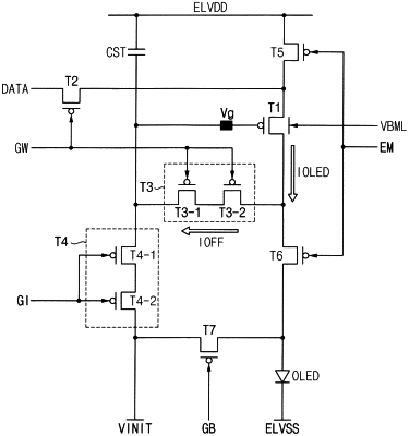
1. A pixel of an organic light emitting diode display device, the pixel comprising:
a first capacitor including a first electrode connected to a wire of a first power supply voltage, and a second electrode connected to a gate node;
a first transistor including a gate electrode connected to the gate node, and a back gate electrode connected to a back gate line through which a back gate voltage is provided;
a second transistor which transmits a data signal to a source of the first transistor in response to a first gate signal;
a third transistor which diode-connects the first transistor in response to the first gate signal;
a fourth transistor which transmits an initialization voltage to the gate node in response to a second gate signal; and
a light emitting diode including an anode, and a cathode connected to a wire of a second power supply voltage,
wherein the first transistor is a driving transistor of the pixel that generates a driving current flowing through the light emitting diode based on the data signal stored in the first capacitor,
wherein the first transistor receives the back gate voltage, which is obtained by delaying the first gate signal by a ½ frame, through the back gate electrode in a low-frequency driving mode, such that distortion of a voltage of the gate node caused by leakage currents of the third and fourth transistors during the low-frequency driving mode is compensated, and
wherein the gate electrode of the first transistor is not connected to the back gate electrode of the first transistor.
|