| CPC G09G 3/32 (2013.01) [G06V 40/1318 (2022.01); G09G 2300/0413 (2013.01); G09G 2300/0809 (2013.01); G09G 2330/028 (2013.01)] | 14 Claims |
|
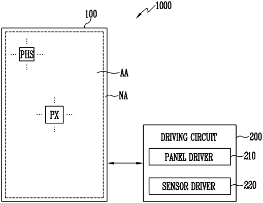
1. A display device comprising:
a plurality of pixel circuits disposed in each of an ith (i is a natural number) pixel row and an (i+1)th pixel row;
a dummy sensor circuit disposed between two pixel circuits located in different columns among the plurality of pixel circuits of the ith pixel row;
a sensor circuit disposed between two pixel circuits located in different columns among the plurality of pixel circuits of the (i+1)th pixel row;
a bank layer disposed on a backplane structure where the plurality of pixel circuits, the dummy sensor circuit, and the sensor circuit are located, and including a plurality of openings;
a plurality of light emitting elements connected to each of the plurality of pixel circuits and disposed in openings corresponding to a light emitting area among the plurality of openings; and
a plurality of light receiving elements connected to the sensor circuit and disposed in openings corresponding to a light receiving area among the plurality of openings,
wherein the dummy sensor circuit is not connected to any of the plurality of light receiving elements.
|