| CPC G09G 3/32 (2013.01) [G09G 2300/0426 (2013.01); G09G 2310/061 (2013.01); G09G 2310/08 (2013.01); G09G 2320/0233 (2013.01); G09G 2320/064 (2013.01)] | 19 Claims |
|
1. A display device comprising:
a display panel comprising a pixel array comprising a plurality of pixels and a plurality of sub-pixel circuits, wherein the plurality of pixels are arranged in a plurality of row lines, each pixel of the plurality of pixels comprises a plurality of inorganic light emitting elements, a sub-pixel circuit of the plurality of sub-pixel circuits is provided for each inorganic light emitting element of the plurality of inorganic light emitting elements and is configured to drive the inorganic light emitting element based on an image data voltage, and each sub-pixel circuit of the plurality of sub-pixel circuits comprises a driving transistor;
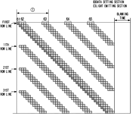
a driver configured to set the image data voltage to sub-pixel circuits in each row line of the plurality of row lines in an order of the row lines, and drive sub-pixel circuits in at least two continued row lines among the plurality of row lines so that inorganic light emitting elements in the at least two continued row lines emit light in the order of the row lines based on the set image data voltage;
a sensing unit configured to sense a current flowing in the driving transistor of each sub-pixel circuit of the plurality of sub-pixel circuits based on a specific voltage applied to the sub-pixel circuit of the plurality of sub-pixel circuits, and output sensing data corresponding to the sensed current; and
a correction unit configured to correct the image data voltage applied to the sub-pixel circuit of the plurality of sub-pixel circuits based on the sensing data,
wherein the driver is further configured to:
set the image data voltage to the sub-pixel circuits in each row line of the plurality of row lines once during a data setting section for each row line of the plurality of row lines, and
drive the sub-pixel circuits in each row line of the plurality of row lines so that inorganic light emitting elements in each row line of the plurality of row lines emit light based on the set image data voltage a number of times during a plurality of light emitting sections for each row line of the plurality of row lines.
|