| CPC G09G 3/2096 (2013.01) [G09G 3/3266 (2013.01); G09G 3/20 (2013.01); G09G 2300/0426 (2013.01); G09G 2310/0267 (2013.01); G09G 2310/0286 (2013.01); G09G 2310/08 (2013.01); G09G 2320/0626 (2013.01); G09G 2330/021 (2013.01); G11C 19/28 (2013.01)] | 18 Claims |
|
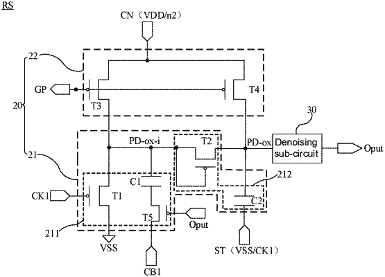
1. A shift register circuit, comprising
a denoising control sub-circuit and a denoising sub-circuit;
wherein the denoising, control sub-circuit is coupled to a first voltage terminal, a first clock signal terminal, a second clock signal terminal and a first denoising control node;
the denoising control sub-circuit is configured to:
generate an alternating voltage signal according to a voltage of the first voltage terminal and a signal of the second clock signal terminal in response to a signal of the first clock signal terminal;
rectify the alternating voltage signal; and
output a signal to the first denoising control node, so that a voltage of the first denoising control node is maintained to be a voltage that enables the denoising sub-circuit to be turned on;
the denoising sub-circuit is coupled to the first denoising control node and a scan signal output terminal; and
the denoising sub-circuit is configured to denoise the scan signal output terminal in response to the voltage of the first denoising control node being the voltage that enables the denoising sub-circuit to be turned on,
wherein the denoising control sub-circuit includes:
a first turn-on control sub-circuit, the first turn-on control sub-circuit being coupled to the first clock signal terminal, the second clock signal terminal, the first voltage terminal, and a second denoising control node, and being configured to output the voltage of the first voltage terminal to the second denoi sing control node periodically in response to the signal of the first clock signal terminal, and to adjust a voltage of the second denoising control node periodically according to the signal of the second clock signal terminal, so that the second denoising control node provides the alternating voltage signal; and
a second turn-on control sub-circuit, the second turn-on control sub-circuit being coupled to the first denoising control node and the second denoising control node and being configured to, in response to the alternating voltage signal provided by the second denoising control node, rectify the alternating voltage signal, and then output the signal to the first denoising control node,
wherein the first turn-on control sub-circuit includes:
a first transistor, a control electrode of the first transistor being coupled to the first clock signal terminal, a first electrode of the first transistor being coupled to the first voltage terminal, and a second electrode of the first transistor being coupled to the second denoising control node;
a first capacitor, a first terminal of the first capacitor being coupled to a second electrode of a fifth transistor, and a second terminal of the first capacitor being coupled to the second denoising control node; and
the fifth transistor, a control electrode of the fifth transistor being coupled to the scan signal output terminal, and a first electrode of the fifth transistor being coupled to the second clock signal terminal; and
the second turn-on control sub-circuit includes:
a second transistor, a control electrode of the second transistor being coupled to the second denoising control node, a first electrode of the second transistor being coupled to the first denoising control node, and a second electrode of the second transistor being coupled to the second denoising control node; and
a second capacitor, a first terminal of the second capacitor being coupled to a first signal terminal, and a second terminal of the second capacitor being coupled to the first denoising control node.
|