| CPC G09G 3/2092 (2013.01) [G09G 3/3233 (2013.01); G09G 3/3266 (2013.01); G09G 2310/0202 (2013.01); G09G 2310/0267 (2013.01); G09G 2310/0275 (2013.01); G09G 2310/0286 (2013.01); G09G 2310/08 (2013.01)] | 9 Claims |
|
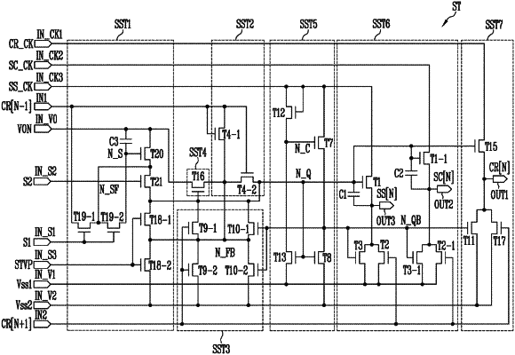
1. A scan driver comprising:
a plurality of stages, each of which is configured to control a voltage of a first node in response to a first signal of a previous stage and to output a second signal in response to the voltage of the first node,
wherein an nth stage, where n is a natural number, from among the plurality of stages comprises:
a first transistor coupled between a first terminal configured to receive the first signal and a second node, the first transistor comprising a gate electrode coupled to a second terminal;
a capacitor coupled between the second node and a third terminal;
a second transistor coupled between the third terminal and a third node, the second transistor comprising a gate electrode coupled to the second node; and
a third transistor coupled between the third node and the first node, the third transistor comprising a gate electrode coupled to a fourth terminal.
|