| CPC G09G 3/20 (2013.01) [G09G 2300/0408 (2013.01); G09G 2310/0267 (2013.01); G09G 2310/08 (2013.01); G09G 2320/0223 (2013.01)] | 20 Claims |
|
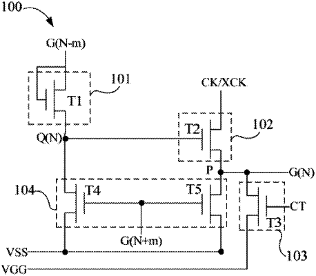
1. A gate driver on array (GOA) circuit, comprising multi-stage cascade GOA units, wherein an N-th stage GOA unit comprises a pull-up control module, a pull-up module, a chamfering control module, and a pull-down module;
the pull-up control module is connected to an (N−m)-th stage scan signal, and is electrically connected to a first node, and the pull-up control module is configured to output the (N−m)-th stage scan signal to the first node under control of the (N−m)-th stage scan signal, wherein N and m are integers greater than zero, and N>m;
the pull-up module is connected to a clock signal and is electrically connected to the first node and an N-th stage scan signal output terminal, and the pull-up module is configured to output the N-th stage scan signal under control of a potential of the first node and the clock signal;
the chamfering control module is connected to a chamfering control signal and a first reference low level signal, and is electrically connected to the N-th scan signal output terminal, and the chamfering control module is configured to pull down a potential of the N-th scan signal under control of the chamfering control signal and the first reference low level signal; and
the pull-down module is connected to an (N+m)-th stage scan signal and a second reference low level signal, and is electrically connected to the first node and the N-th stage scan signal output terminal, and the pull-down module is configured to pull down the potential of the first node and the potential of the N-th stage scan signal after the chamfering control module pulls down the potential of the N-th stage scan signal under control of the (N+m)-th stage scan signal and the second reference low level signal;
wherein the pull-down module comprises a fourth transistor and a fifth transistor;
the fourth transistor comprises a first terminal, a second terminal, and a third terminal, the fifth transistor comprises a first terminal, a second terminal, and a third terminal, both the first terminal of the fourth transistor and the first terminal of the fifth transistor are connected to the (N+m)-th stage scan signal, the second terminal of the fourth transistor and the second terminal of the fifth transistor are connected to the second reference low level signal, and the third terminal of the fourth transistor and the third terminal of the fifth transistor are electrically connected to the first node.
|