| CPC G06V 40/1318 (2022.01) [G06F 3/041 (2013.01)] | 11 Claims |
|
1. An electronic device comprising:
a control portion;
a memory portion; and
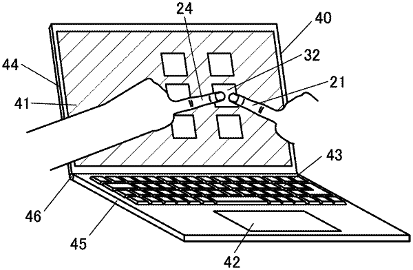
a display portion comprising a plurality of pixels, each of the plurality of pixels comprising a light-emitting element and a light-emitting and light-receiving element,
wherein the display portion is configured to display a first icon and concurrently obtain first fingerprint data of a plurality of users in a display region of the first icon,
wherein the memory portion is configured to retain second fingerprint data of users registered in advance, and
wherein the control portion is configured to compare the first fingerprint data with the second fingerprint data; execute first processing associated with the first icon in the case where the first fingerprint data and the second fingerprint data match; and execute second processing in the case where the first fingerprint data and the second fingerprint data do not match.
|