| CPC G06F 7/5443 (2013.01) [H03K 5/26 (2013.01); G06N 3/063 (2013.01); H02J 7/345 (2013.01); H03K 19/21 (2013.01)] | 15 Claims |
|
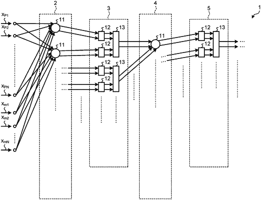
1. A signal processing circuit, comprising:
a plurality of first circuits each including a first time-length signal output circuit and a second time-length signal output circuit, wherein
the first time-length signal output circuit is configured to output a first time-length signal representing a time length between first timing at which a first input signal changes and second timing at which a second input signal changes, and
the second time-length signal output circuit is configured to output the first time-length signal as a second time-length signal at timing based on a control signal; and
a second circuit configured to output the second time-length signal having the longest time length among a plurality of second time-length signals output respectively from the plurality of first circuits.
|