| CPC G06F 3/0659 (2013.01) [G06F 12/0246 (2013.01); G06F 12/06 (2013.01); G11C 7/1063 (2013.01); G11C 7/109 (2013.01); G11C 16/06 (2013.01); G11C 16/08 (2013.01); G11C 16/12 (2013.01); G11C 16/26 (2013.01)] | 18 Claims |
|
1. A memory system comprising:
a memory device; and
a memory controller,
wherein the memory device comprises:
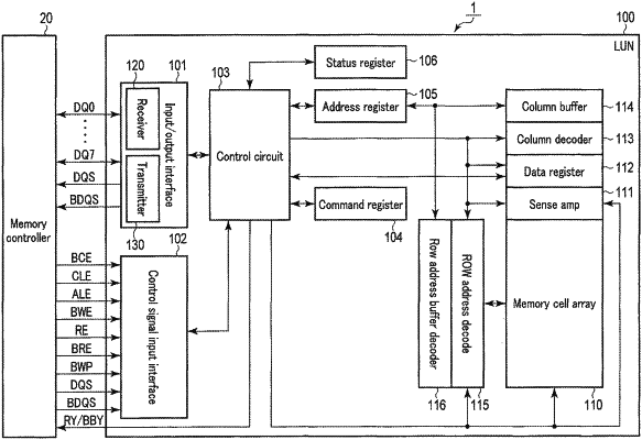
a memory cell array configured to store data;
a data input and output interface configured to receive a command, an address, and data to be written into the memory cell array from the memory controller, and to output data read from the memory cell array to the memory controller;
a command register configured to store a command sent from the memory controller;
an address register configured to store an address sent from the memory controller;
a transmitter connected to the data input and output interface and configured to be driven with an enable signal; and
a control circuit configured to cause the memory cell array to perform a read operation in response to receipt of a read command while a first control signal is being asserted by the memory controller and receipt of a read address subsequent to the read command while a second control signal is being asserted by the memory controller,
wherein the memory controller concurrently asserts the first control signal and the second control signal before sending the read command to cause the control circuit of the memory device to bring the enable signal to a first level and maintain the enable signal at the first level at least until after the read command is received,
wherein the first control signal comprises a signal for causing the command register to store the command,
wherein the second control signal comprises a signal for causing the address register to store the address, and
wherein, in the memory device, the enable signal is brought to the first level based on a first logical operation result, the first logical operation being a logical operation between a command and a second logical operation result, and the second logical operation result being a logical operation between the first control signal and the second control signal.
|