| CPC G06F 3/0655 (2013.01) [G06F 3/0604 (2013.01); G06F 3/0679 (2013.01)] | 16 Claims |
|
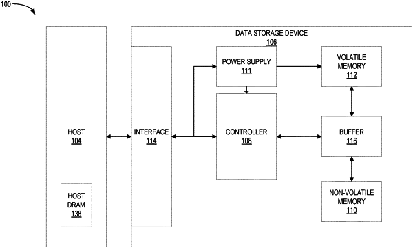
1. A data storage device, comprising:
a memory device; and
a controller coupled to the memory device, the controller configured to:
set first default link attributes to a first frequency at a first power on, wherein the first default link attributes is a pulse width modulation (PWM) link startup sequence (LSS);
receive a host reference clock signal from a host device, wherein the host reference clock signal has a second frequency and second default link attributes different from the first default link attributes, wherein the second default link attributes is a high speed (HS) LSS;
determine that the second frequency is higher than the first frequency;
ignore the first frequency;
operate at the second frequency while maintaining the first default link attributes; and
change from the first default link attributes to the second default link attributes at a second power on.
|