US 12,001,698 B2
Memory system and SoC including linear address remapping logic
Dongsik Cho, Yongin-si (KR)
Assigned to Samsung Electronics Co., Ltd., (KR)
Filed by Samsung Electronics Co., Ltd., Suwon-si (KR)
Filed on Feb. 6, 2023, as Appl. No. 18/105,967.
Application 18/105,967 is a continuation of application No. 17/155,503, filed on Jan. 22, 2021.
Application 17/155,503 is a continuation of application No. 16/983,389, filed on Aug. 3, 2020, granted, now 11,681,449.
Application 16/983,389 is a continuation of application No. 16/940,687, filed on Jul. 28, 2020, granted, now 11,573,716.
Application 16/940,687 is a continuation of application No. 16/215,827, filed on Dec. 11, 2018, granted, now 11,169,722, issued on Nov. 9, 2021.
Application 16/215,827 is a continuation of application No. 15/424,019, filed on Feb. 3, 2017, granted, now 10,817,199, issued on Oct. 27, 2020.
Application 15/424,019 is a continuation of application No. 14/990,975, filed on Jan. 8, 2016, abandoned.
Application 14/990,975 is a continuation of application No. 13/803,269, filed on Mar. 14, 2013, granted, now 9,256,531, issued on Feb. 9, 2016.
Claims priority of application No. 10-2012-0065624 (KR), filed on Jun. 19, 2012.
Prior Publication US 2023/0185466 A1, Jun. 15, 2023
This patent is subject to a terminal disclaimer.
Int. Cl. G06F 3/06 (2006.01); G06F 12/02 (2006.01); G06F 12/06 (2006.01); G06F 15/78 (2006.01); G06F 13/42 (2006.01)
CPC G06F 3/0634 (2013.01) [G06F 3/0604 (2013.01); G06F 3/0611 (2013.01); G06F 3/0625 (2013.01); G06F 3/0638 (2013.01); G06F 3/0673 (2013.01); G06F 3/0683 (2013.01); G06F 12/02 (2013.01); G06F 12/0607 (2013.01); G06F 15/781 (2013.01); G06F 12/0646 (2013.01); G06F 13/4282 (2013.01); G06F 2212/1016 (2013.01); G06F 2212/1024 (2013.01); G06F 2212/1028 (2013.01); Y02D 10/00 (2018.01)] 17 Claims
OG exemplary drawing
 
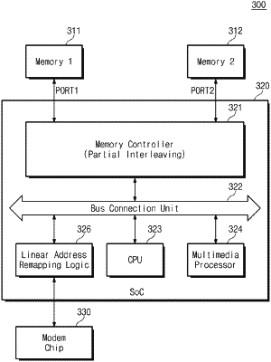
1. A system-on-chip comprising:
a first memory port;
a second memory port;
a memory controller configured to access a first memory device through the first memory port or a second memory device through the second memory port;
a processor configured to generate memory addresses for accessing a memory region and configured to generate a control signal for selecting a linear mode and a interleave mode, and, when the memory addresses are greater than a base address, the processor generates the control signal such that the linear mode is selected; and
an address remapping logic configured to, in the linear mode, remap the memory addresses into remapped addresses based on the control signal,
wherein the memory controller is further configured to, in the linear mode, perform a first linear access operation on a first region of the memory region by accessing only the first memory device through the first memory port in response to first remapped addresses of the remapped addresses.