| CPC G06F 3/0613 (2013.01) [G06F 3/0656 (2013.01); G06F 3/0679 (2013.01)] | 20 Claims |
|
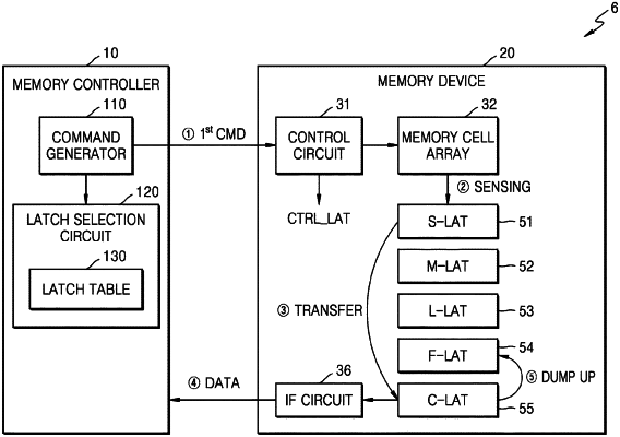
1. A memory system comprising:
a memory device comprising:
a memory cell array connected to a plurality of bit lines;
a first latch configured to sense data stored in the memory cell array;
a plurality of program latches configured to store data which is to be programmed in the memory cell array, or data which determines a voltage level pre-charged in the plurality of bit lines in performing a program operation; and
a second latch configured to receive data which is to be programmed in the memory cell array, or output data sensed from the memory cell array; and
a memory controller configured to provide a command to the memory device,
wherein the memory device is configured to:
sense first data from a first region of the memory cell array,
store the first data in the first latch,
transfer the first data from the first latch to the second latch,
output the first data from the second latch to the memory controller, and
in response to a first read command, transfer the first data from the second latch to a first program latch of the plurality of program latches.
|