| CPC G06F 3/0607 (2013.01) [G06F 3/0632 (2013.01); G06F 3/0655 (2013.01); G06F 3/0679 (2013.01); G06F 3/0688 (2013.01)] | 5 Claims |
|
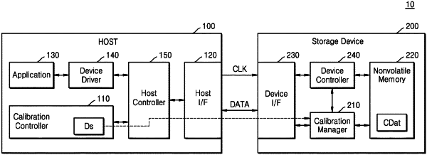
1. A Universal Flash Storage (UFS) device communicably connected to a host, the UFS device comprising:
a device interface connected to the host configured to exchange data and commands with the host and include a link layer and a PHY layers;
a flash memory configured to store calibration data of the host; and
a device controller comprising:
a central processing unit (CPU);
a flash translation layer(FTL);
a flash manager configured to store the data in a selected address of the flash memory by referring to address mapping information of the FTL;
a command manager configured to receive the commands via the device interface;
a calibration manager configured to receive a descriptor in a command received from the host including setting information, update the calibration data with the setting information via the CPU, the FTL and the flash manager, and change a setting value of a register included in the link layer and the PHY layer based on the updated calibration data.
|