| CPC G06F 13/1668 (2013.01) [G06F 13/28 (2013.01)] | 20 Claims |
|
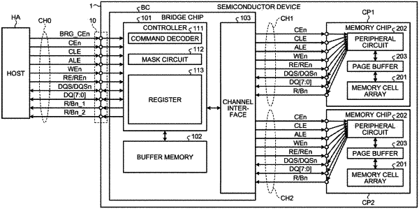
1. A semiconductor device comprising:
a terminal group configured to receive a first signal and a second signal from a host;
a first chip electrically connected to the terminal group and configured to receive the first signal and the second signal; and
a second chip electrically connected to the first chip and configured to receive a third signal from the first chip, the third signal corresponding to the first signal,
wherein the first chip is configured to:
transmit the third signal to the second chip by the first chip receiving the first signal, and
refrain from transmitting the third signal to the second chip by the first chip receiving the second signal before the first chip receiving the first signal.
|