| CPC G06F 12/0842 (2013.01) [G11C 16/0483 (2013.01); G11C 16/08 (2013.01); G11C 16/10 (2013.01); G11C 16/24 (2013.01); G11C 16/30 (2013.01); G11C 16/3459 (2013.01); G06F 2212/1024 (2013.01)] | 20 Claims |
|
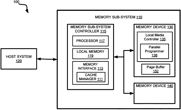
1. A memory device comprising:
a page buffer comprising a cache register and multiple data registers;
a memory array comprising a set of sub-blocks coupled with the page buffer, wherein the set of sub-blocks comprises memory cells configured as single-level cell (SLC) memory; and
control logic operatively coupled with the page buffer, the control logic to perform operations comprising:
causing a first page of SLC data to be stored in the cache register;
causing the first page of the SLC data to be moved from the cache register to a first data register of the multiple data registers;
causing a subsequent page of the SLC data to be stored in the cache register;
causing the subsequent page and the first page of the SLC data stored in the cache register and in the first data register, respectively, to be concurrently programmed to the set of sub-blocks, wherein the first page is programmed to a first sub-block and the subsequent page is programmed to a subsequent sub-block of the set of sub-blocks; and
causing the operations for programming the set of sub-blocks to be performed in parallel.
|